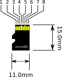
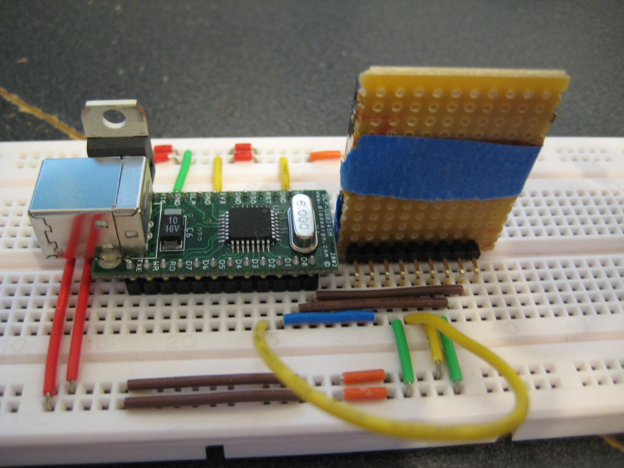
 If you're looking for a run down of the features and history of SD or microSD cards, go read the appropriate Wikipedia article (here and here). This page is just going to concern itself with attached these fingernail-sized chunks of storage to commodity microcontrolers.
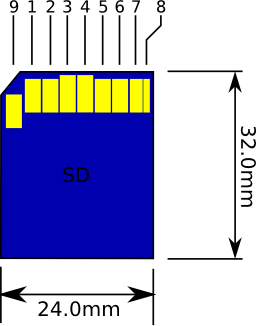 |
|
|||||||||||||||||||||||||||||||||||||||||||||||||||||||||||||||||||||||||||||||||||
 |
|
|||||||||||||||||||||||||||||||||||||||||||||||||||||||||||||||||||||||||||||||||||
| Type | MMC | SD | microSD |
|---|---|---|---|
| SPI Mode | Optional | Yes | Optional |
| 1 bit mode | Yes | Yes | Yes |
| 4 bit mode | No | Optional | Optional |
| Xfer clock | 0–20 MHz | 0–25 MHz - 0–50 MHz | 0–25 MHz? |
| Max Transfer | 20 Mbit/s | 100 Mbit/s - 200 Mbit/s | 100 Mbit/s |
| Max SPI Transfer | 20 Mbit/s | 25 Mbit/s | 25 Mbit/s |
| DRM Aval. | No | Yes | Yes |

| Start Bit | Transmission Bit | Command Bit Pattern | Argument | CRC7 | End Bit | |
|---|---|---|---|---|---|---|
| Bit position | 47 | 46 | [45:40] | [39:8] | [7:1] | 0 |
| Width (Bits) | 1 | 1 | 6 | 32 | 7 | 1 |
| Value | 0 | 1 | 1 |
| CMD INDEX | Bit Pattern | Mnemonic | Argument | Response Format | Command Description |
|---|---|---|---|---|---|
| CMD0 | 000000 | GO_IDLE_STATE | [31:0] Stuff Bits | R1 | Resets the SD Memory Card |
| CMD1 (note 1) | 000001 | SEND_OP_COND | [31] Reserved [30] HCS [29:0] Reserved |
R1 | Sends host capacity support information and activates the card's initialization process. HCS is effective when card receives SEND_IF_COND command. Reserved bits shall be set to '0'. |
| CMD6 (note 8) | SWITCH_FUNC | [31] Mode (0 = Check function, 1 = Switch function) [30:24] reserved (All ’0’) [23:20] reserved for function group 6 (All ’0’ or 0xF) [19:16] reserved for function group 5 (All ’0’ or 0xF) [15:12] reserved for function group 4 (All ’0’ or 0xF) [11:8] reserved for function group 3 (All ’0’ or 0xF) [7:4] function group 2 for command system [3:0] function group 1 for access mode |
R1 | Checks switchable function (mode 0) and switches card function (mode 1). See Chapter 4.3.10 of the Physical Layer Simplified Spec. |
|
| CMD8 (note 9) | 001000 | SEND_IF_COND | [31:12] Reserved Bits [11:8] Supply voltage (VHS) [7:0] Check Pattern |
R7 | Sends SD Memory Card interface condition that includes Host Supply Voltage (VHS) information and asks the accessed card whether card can operate in supplied voltage range. Reserved bits shall be set to '0'. |
| CMD9 | SEND_CSD | [31:0] Stuff Bits | R1 | Asks the selected card to send its card-specific data (CSD) | |
| CMD10 | SEND_CID | [31:0] Stuff Bits | R1 | Asks the selected card to send its card identification (CID) | |
| CMD12 | STOP_TRANSMISSION | [31:0] Stuff Bits | R1b (note 5) | Forces the card to stop transmission in Multiple Block Read Operation | |
| CMD13 | SEND_STATUS | [31:0] Stuff Bits | R2 | Asks the selected card to send its status register. | |
| CMD16 | 010000 | SET_BLOCKLEN | [31:0] Block Length | R1 | Sets a block length (in bytes) for all following block commands (read and write) (note 2) of a Standard Capacity Card. Block length of the read and write commands are fixed to 512 bytes in SDHC and SDXC cards. The length of LOCK_UNLOCK command is set by this command in all cards, regardless of capacity. |
| CMD17 | READ_SINGLE_BLOCK | [31:0] Data Address (note 10) | R1 | Reads a block of the size selected by SET_BLOCKLEN command (note 3) | |
| CMD18 | READ_MULTIPLE_BLOCK | [31:0] Data Address (note 10) | R1 | Continuously transfers data blocks from card to host until interrupted by a STOP_TRANSMISSION command. | |
| CMD24 | WRITE_BLOCK | [31:0] Data Address (note 10) | R1 | Writes a block of the size selected by the SET_BLOCKLEN command. (note 4) | |
| CMD25 | WRITE_MULTIPLE_BLOCK | [31:0] Data Address (note 10) | R1 | Continuously writes blocks of data until 'Stop Tran' token is sent (instead of 'Start Block'). | |
| CMD27 | PROGRAM_CSD | [31:0] Stuff Bits | R1 | Programming of the programmable bits of the CSD. | |
| CMD28 | SET_WRITE_PROT | [31:0] Data Address | R1b (note 5) | If the card has write protection features, this command sets the write protection bit of the addressed group. The properties of write protection are coded in the card specific data (WP_GRP_SIZE). SDHC and SDXC cards do not support this command. |
|
| CMD29 | CLR_WRITE_PROT | [31:0] Data Address | R1b (note 5) | If the card has write protection features, this command clears the write protection bit of the addressed group. SDHC and SDXC cards do not support this command. |
|
| CMD30 | SEND_WRITE_PROT | [31:0] Write protect data address | R1 | If the card has write protection features, this command asks the card to send the status of the write protection bits. (note 6) SDHC and SDXC cards do not support this command. |
|
| CMD32 | ERASE_WR_BLK_START_ADDR | [31:0] Data Address (note 10) | R1 | Sets the address of the first write block to be erased. | |
| CMD33 | ERASE_WR_BLK_END_ADDR | [31:0] Data Address (note 10) | R1 | Sets the address of the last write block of the continuous range to be erased. | |
| CMD38 | ERASE | [31:0] Stuff Bits | R1b (note 5) | Erases all previously selected write blocks | |
| CMD42 | LOCK_UNLOCK | [31:0] Reserved bits (set all to 0) | R1 | Used to Set/Reset the Password or lock/unlock the card. A transferred data block includes all the command details - refer to Chapter 4.3.7 of the Physical Layer Simplified Spec v3.01. The size of the Data Block is defined with SET_BLOCK_LEN command. Reserved bits in the argument and in Lock Card Data Structure shall be set to 0. |
|
| CMD55 | APP_CMD | [31:0] Stuff Bits | R1 | Defines to the card that the next command is an application specific command rather than a standard command. | |
| CMD56 | GEN_CMD | [31:1] Stuff Bits [0] RD/WR (note 7) |
R1 | Used either to transfer a Data Block to the card or to get a Data Block from the card for general purpose/application specific commands. In case of Standard Capacity SD Memory Card, the size of the Data Block shall be defined with SET_BLOCK_LEN command. Block length of this command is fixed to 512-byte in SDHC and SDXC cards. | |
| CMD58 | READ_OCR | [31:0] Stuff Bits | R3 | Reads the OCR register of a card. CCS bit is assigned to OCR[30]. | |
| CMD59 | CRC_ON_OFF | [31:1] Stuff Bits [0] CRC option |
R1 | Turns the CRC option on or off. A '1' turns the option on, a '0' will turn it off. |
| ACMD INDEX | Bit Pattern | Mnemonic | Argument | Response Format | Command Description |
|---|---|---|---|---|---|
| ACMD13 | SD_STATUS | [31:0] Stuff Bits | R2 | Send the cards status register. Note: The spec says that the card (in SPI mode) will respond with an R2 token, but also states it will return the fields in Table 4-38 (of the Physical Layer Simplified Spec v3.01) - which is a 512 bit block. |
|
| ACMD22 | SEND_NUM_WR_BLOCKS | [31:0] Stuff Bits | R1 | Send the numbers of the well written (without errors) blocks. Responds with 32-bit+CRC data block. | |
| ACMD23 | SET_WR_BLK_ERASE_COUNT | [31:23] Stuff Bits [22:0] Number of blocks |
R1 | Set the number of write blocks to be pre-erased before writing (to be used for faster Multiple Block WR command). '1'=default (one wr block) (note 2). |
|
| ACMD41 | SD_SEND_OP_COND | [31] Reserved Bit [30] HCS [29:0] Reserved Bits |
R1 | Sends host capacity support information and activates the card's initialization process. Reserved bits shall be set to '0'. |
|
| ACMD42 | SET_CLR_CARD_DETECT | [31:1] Stuff Bits [0] set_cd |
R1 | Connect ('1')/Disconnect ('0') the 50 KOhm pull-up resistor on CS (pin 1) of the card. The pull-up may be used for card detection. | |
| ACMD51 | SEND_SCR | [31:0] Stuff Bits | R1 | Reads the SD Configuration Register (SCR). |
| Bit | ||
|---|---|---|
| 0 | In idle state | The card is in idle state and running the initializing process. |
| 1 | Erase reset | An erase sequence was cleared before executing because an out of erase sequence command was received. |
| 2 | Illegal command | An illegal command code was detected. |
| 3 | Communication CRC error | The CRC check of the last command failed. |
| 4 | Erase sequence error | An error in the sequence of erase commands occurred. |
| 5 | Address error | A misaligned address that did not match the block length was used in the command. |
| 6 | Parameter error | The command’s argument (e.g. address, block length) was outside the allowed range for this card. |
| 7 | MSB | Always Zero |
| Bit | ||
|---|---|---|
| 0 | Card is locked | Set when the card is locked by the user. Reset when it is unlocked. |
| 1 | Write protect erase skip | lock/unlock command failed | This status bit has two functions overloaded. It is set when the host attempts to erase a write-protected sector or makes a sequence or password errors during card lock/unlock operation. |
| 2 | Error | A general or an unknown error occurred during the operation. |
| 3 | CC error | Internal card controller error. |
| 4 | Card ECC failed | Card internal ECC was applied but failed to correct the data. |
| 5 | Write protect violation | The command tried to write a write-protected block. |
| 6 | Erase param | An invalid selection for erase, sectors or groups. |
| 7 | out of range | csd overwrite |
